Photovoltaics Research Laboratory
Innovation. Development. Demonstration.
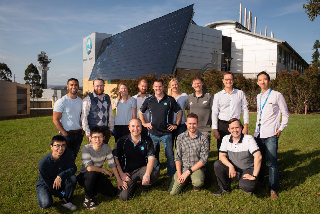
Our photovoltaic research activities cover the entire technology chain including new materials discovery, device fabrication and optimisation, materials characterisation and cell performance determination, energy yield and device durability. Our Photovoltaics Team members have a collective 50+ year history in the development of new device technologies.
Standard Photovoltaics Characterisation Facility
NATA accredited cell testing
Our Photovoltaics Performance Laboratory (PVPL) includes a solar cell measurement laboratory; it’s the only PV laboratory in the southern hemisphere to achieve National Association of Testing Authorities (NATA) accreditation for the IEC17025 technical competency standard. This makes us one of the most accurate laboratories in the world for measuring photovoltaic efficiency.
Our cell measurement laboratory forms part of the CSIRO Photovoltaics Research Laboratory at the National Solar Energy Centre, established in 2006. CSIRO has invested in the investigation of photovoltaics including next generation solar cell technologies. Our research facilities including world class equipment for the assessment, development and prototyping of emerging photovoltaic technologies for a growing renewable energy market.
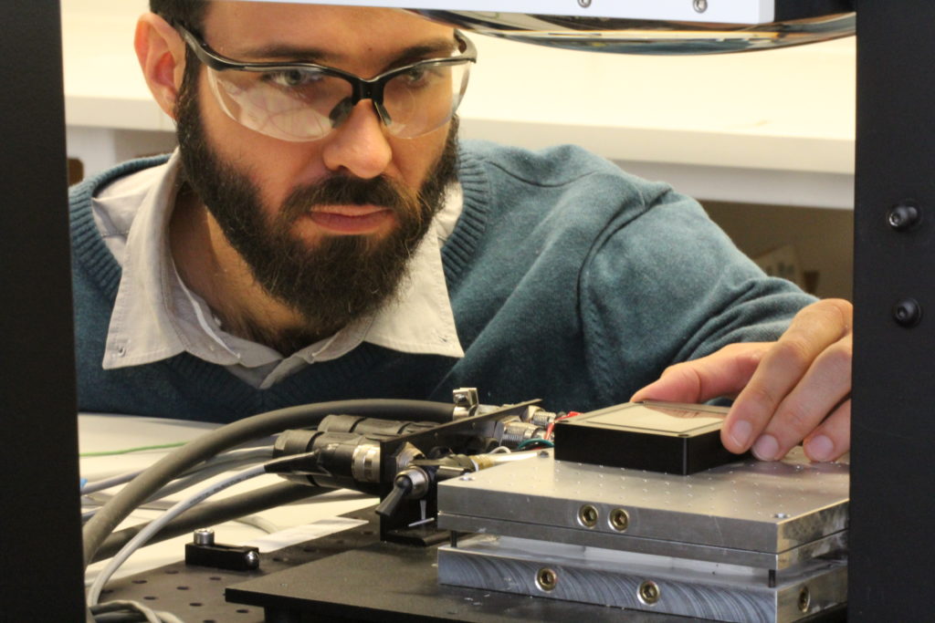
Dr Ricky Dunbar aligning a reference cell under test
Next Generation Perovskite Photovoltaics
Using crystalline materials similar to silicon as a semiconductor
We’re leading the Next Generation of solar cells using perovskite semiconductors, based on an organic-inorganic structure, which are a new form of crystalline semiconductor. They have unique electronic properties, typically fabricated using solution processed techniques.
As a photovoltaic material, they afford high cell efficiency at low market entry cost with a projected future manufacturing price estimated at < $0.25/W. Perovskite semiconductors share a complex chemistry for optimisation like other thin-film quaternary semiconductors such as copper-indium-gallium-selenide or CIGS cells.
Perovskite semiconductors are based around an ABX3 crystal structure. These are structurally similar to the mineral form of these materials and referred to as ‘Perovskite’.
CSIRO has developed and patented a scalable deposition process that can be applied using current industry manufacturing equipment. This technique provides a significant shift from solution processes, and can be applied to transparent conducting oxide glass and other semiconductor surfaces including the formation of multi-junction device configurations.
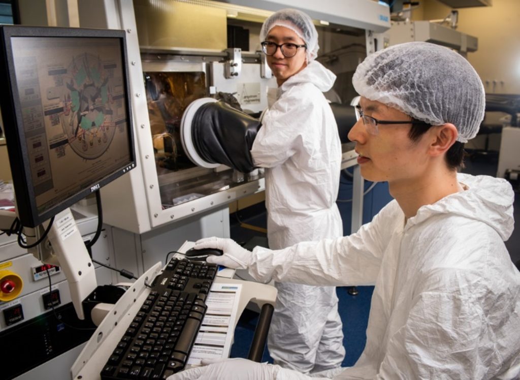
Dr Jacob Wang and Dr Liangyou Lin configuring experimental conditions for deposition of metallic electrode contacts
Our research team and established capabilities afford us many competitive aspects:
- Pre-prototype testing of high performance solar cells
- Accurate cell performance determination
- Laboratory and field experiment test-beds for lifetime and durability
- Thin film deposition, optical and physical characterisation
- Modelling of device performance parameters and correlation to cell design for trouble shooting.
Partner with us.
We are seeking industrial partners to transfer our R&D from laboratory breakthrough to commercial success. If you have any questions, please contact Dr Greg Wilson, the Research Group Leader at Gregory.Wilson@csiro.au.