Next Generation Photovoltaics
Current solar cell technologies are mostly based on silicon wafers: around ~95% of the 100GWp of solar panels produced annually are made with silicon. For silicon wafers, the world-record for light power-to-electrical conversion efficiency (the ability to convert sunlight into electricity) for single-junction cells is now 26.7%. In industry that translates to commercial silicon solar modules at around 20-22% power conversion efficiency (PCE).
Our challenge is to identify new ways of harvesting energy from the sun that are highly efficient, cost‑effective and create a valuable manufacturing proposition for a global market.
We’re researching perovskite semiconductors and multi-junction devices
Metal-halide perovskite structures have emerged as an inexpensive and revolutionary family of photoactive semiconductors in thin-film photovoltaics and one of the most highly investigated topics in high-impact publications.
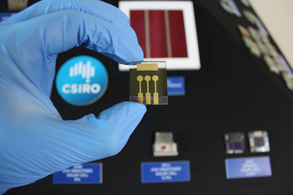
Recently, new perovskite semiconductors have emerged as an inexpensive and revolutionary family of photovoltaic (PV) materials. We call our perovskite-based technology NexGen Solar®. The simple fabrication process of perovskite-based devices, achieving record efficiencies of 25.2% PCE, and their compatibility with other materials, put them in a unique position to penetrate an expanding global PV market.
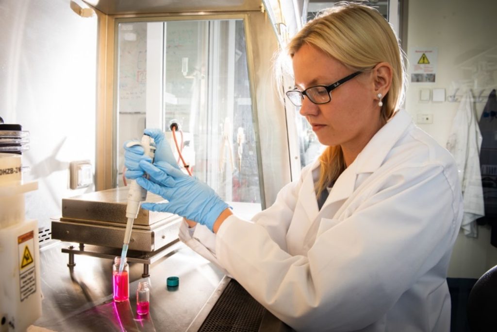
Camilla Lian working under clean room conditions in our humidity controlled laboratory to prepare pre-cursor solutions for device fabrication
NexGen Solar®
CSIRO has developed and patented a novel deposition process for the formation of a low-temperature crystalline semiconductor with remarkable optoelectronic properties. The photoactive material, an organic-inorganic semiconductor in a crystalline phase called ‘perovskite’, has high-electronic charge mobility properties that enable the formation of photoactive devices including application in photovoltaics (solar cells), light-emitting diodes (LEDs), focused emission sources (lasers) and high energy sensors (X-ray, neutron, gamma detectors).
Our research team is investigating new device design and processes to increase the performance of prototype NexGen Solar® cells and modules. We focus on fabricating and measuring thin-film photovoltaic devices, with an emphasis on perovskite semi-conductors as a photoactive material in single- and tandem-junction devices.
The incorporation of NexGen Solar® as the top-junction in a two-junction perovskite-silicon tandem stack operating in normal sunlight can achieve PCE up to 39%. Often the surface of a silicon wafer is textured and effective in reduction of parasitic reflections, improving light absorption and converting more light to electricity. A truly effective tandem device will limit any interference with or incorporate a textured surface, ideally through a conformal coating which is made possible with the CSIRO NexGen Solar® technology.
The NexGen Solar® technology is based on vapour-deposition techniques that are practically ubiquitous across a multitude of industries around the world. Unlike solution-based processes, methods such as chemical vapour deposition, physical vapour deposition and atomic layer deposition have been heavily refined for cost/performance and are compatible with existing PV manufacturing lines.
Partner with us.
We are seeking industrial partners to transfer our R&D from laboratory breakthrough to commercial success. If you have any questions, please contact Dr Greg Wilson, the Research Group Leader at Gregory.Wilson@csiro.au.